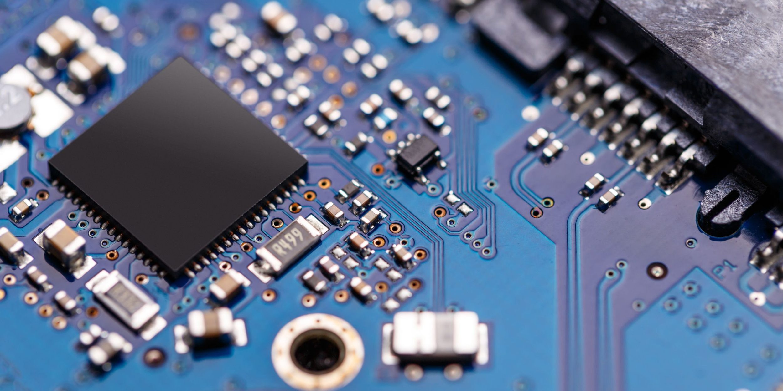
Each year, Americans dispose of around 220 million tons of old electronic devices and computers, the majority thrown away in order to upgrade. This is good news for manufacturers. Devices with printed circuit boards are in high demand. Not just in the U.S., but around the world!
PCBs are essential to the success of your product as are engineering and consulting services. Printed circuit boards bring your device to life by connecting components with circuits and copper traces. Physical board constraints such as materials, size, planes, layers, and connectivity influence these factors. To design a PCB, you must take mechanical and electrical constraints into consideration before laying out your board for its desired fit, form, and function. Design and engineering services can help you get the results you want.
Common PCB Manufacturing Issues
The most common PCB pitfalls can be prevented. You should avoid the following issues:
- Not Enough Copper-to-Edge Clearance – If you trim an edge-piece too close, you may remove the cover and expose the copper layer. This cover is the piece that is supposed to protect the copper from corroding. When you leave enough space between the edge of the board and the edge of the copper, you’ll reduce the risk of shorts during depanelization.
- Plating Voids – Plating voids happen when there are imperfections in the copper-coated holes of a PCB. The purpose of these holes is to allow current to travel from one side of the board to the other. They become ineffective if the depositions are imperfect, are contaminated, or have an air bubble. You can help identify potential issues by cleaning the copper material after drilling the holes.
- Acid Traps – Acute angles that can trap acid during the etching process are called acid traps. They can make the circuit defective by compromising the connection. Always double check your design to make sure it doesn’t include acute angles, especially when working with thin traces.
- Slivers – Occurring during the etching process, slivers can negatively affect the PCB’s function. They are created in one of two ways. First, by cutting an area of the board too thinly or too deep, causing a sliver of material to break away. Second, by using strips of solder mask or copper that are too thin which then detach before liquifying and contaminating the chemical bath. You must design your sections with minimum widths in order to reduce the chances of making slivers.
- Insufficient Solder Mask Dams – Floating parts, solder bridges, and tombstoning can all lead to assembly issues, so it’s important to verify solder mask openings in your design. By doing so, you can help avoid solder shorts between fine pitch leads.
- Electromagnetic Interference (EMI) – Ensuring that circuits perform optimally is imperative. Good practices to employ are proper stack-up design, good grounding, and shielding sensitive traces from noisy signals.
What a Quality Engineering Service Can Do for You
Your company needs specialized technicians to lay out your PCB utilizing the best practices. Our design and engineering services aid development through the use of computers and manufacturing software that identifies design issues and errors while making the best use of the printed circuit board. We know every PCB is different, but there are general accepted practices for PCB layout in each development stage. Our quality engineering service experts and their software help provide the crucial first-steps leading to a template and finished product that work.


